PCB Fabrication
Makerspace 4 - PCB Fabrication
In this makerspace project I created a UV LED light box controlled by an ESP32 to create PCBs (Printed Circuit Boards). This would allow me to manufacture PCBs for cheaper then getting them professionally made. I also learned how to use KiCad and designed my own PCB for an ATTINY85 game console.
The Plan:
I had seen someone online fabricate PCBs at their house and I wanted to try making my own. Since the overall theme of this makerspace was “game” I wanted to create a small game console powered by an ATTINY85 chip.
I first started out by creating a slideshow with everything I would need in the PCB fabrication process. The slideshow and printable list can be found here and here.
The main machine I would need is a UV light box for exposing the PCB photoresist.
The UV Light Box (Structure):
I started the UV light box in cad. I created a simple box that I could mount everything to.
After it was designed I cut the box out of some plywood I found in my garage. I then put the box together with pocket screws.
The box structure was finished with a layer of black paint.
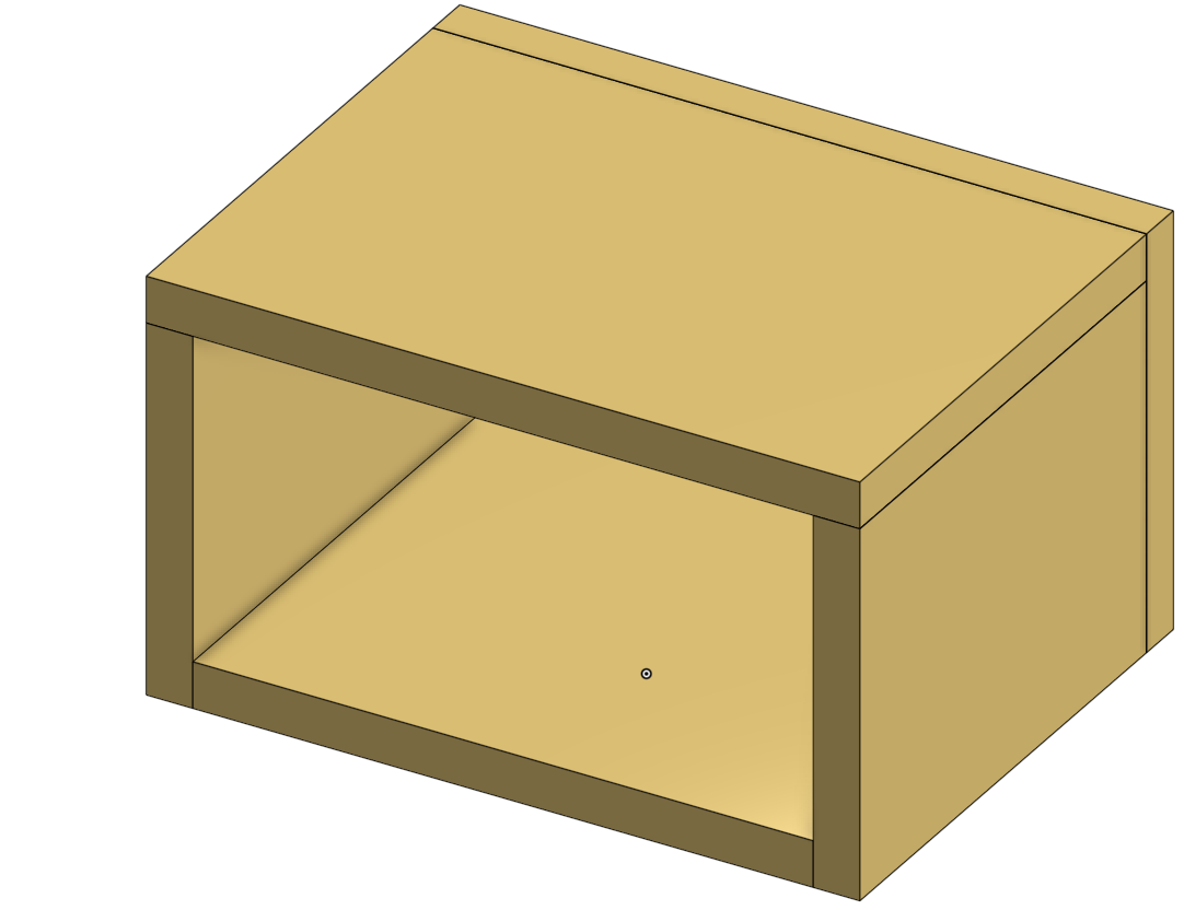
The box in CAD (Onshape).
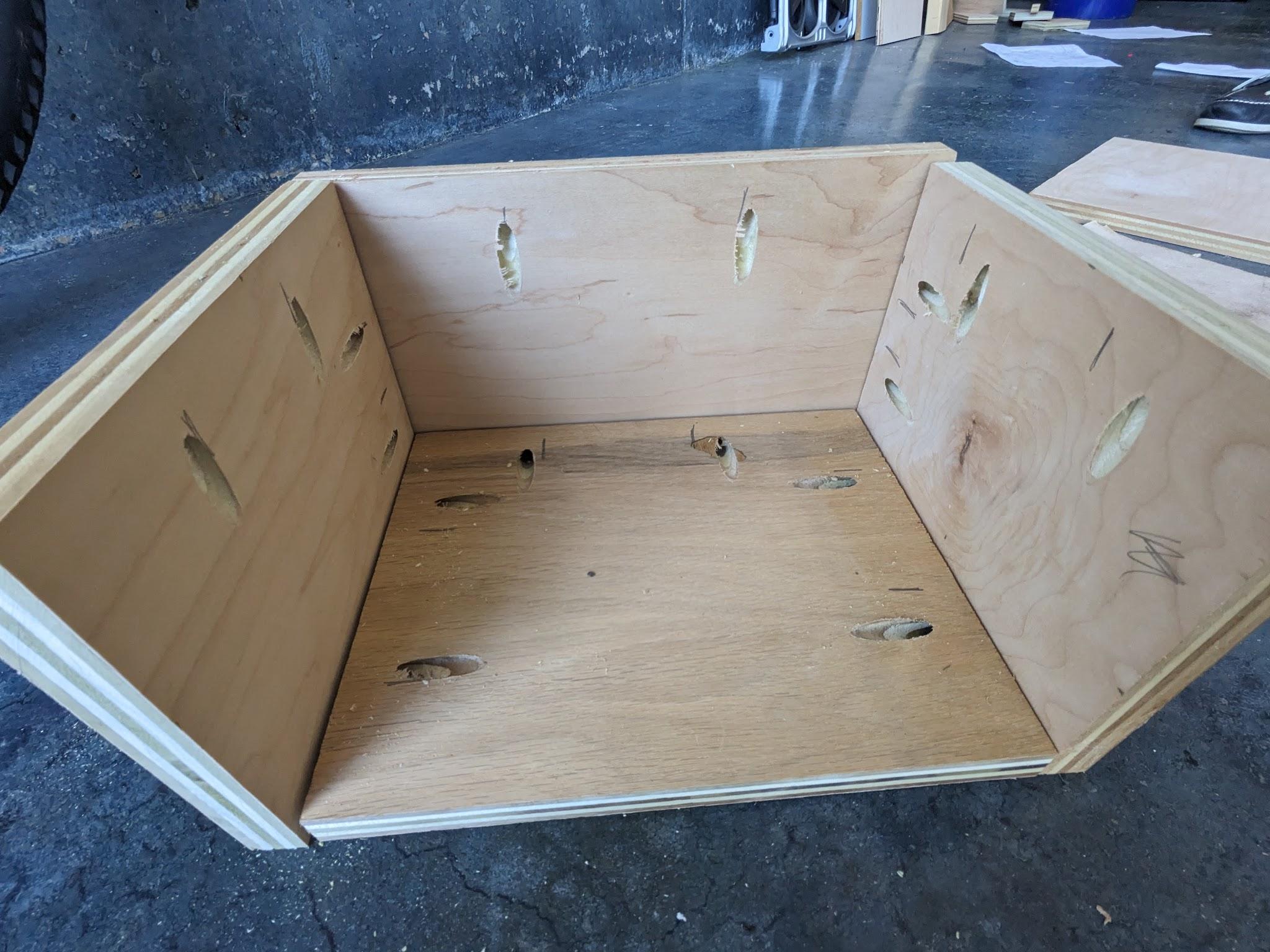
The bottom section of the box.
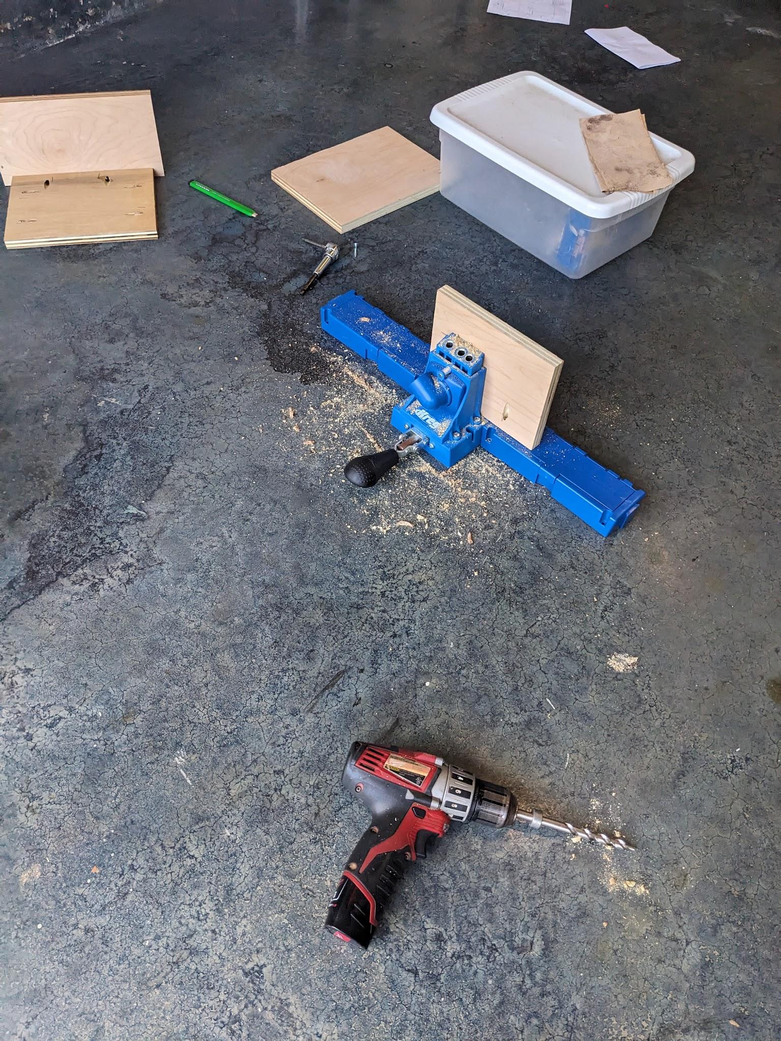
Drilling holes for pocket screws.
Black paint under the UV Light.
The UV Light Box (Electronics):
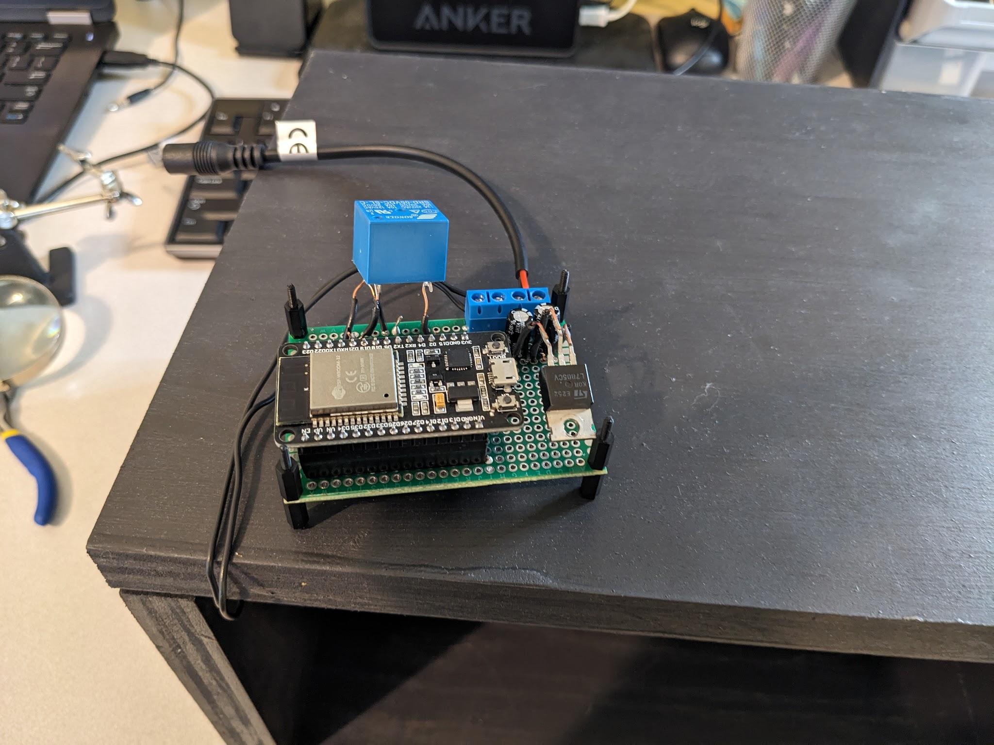
The electronics design for this was a bit tedious as the ESP32 I chose for this project only outputs 3.3v on its GPIO pins (I didn't know this at the start).
I started by designing the circuit to use what I thought was a MOSFET that I found in some scrap electronics I had. I would have used the MOSFET to allow the ESP32 to control the 12v lights.
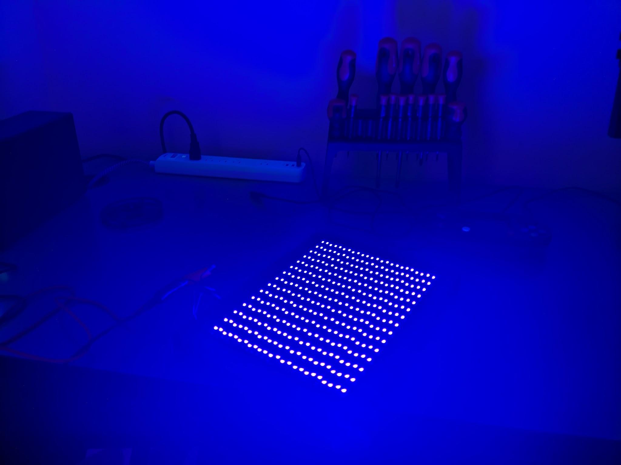
(The UV light gets seen a lot more on camera then in person.)
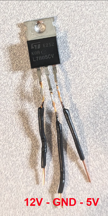
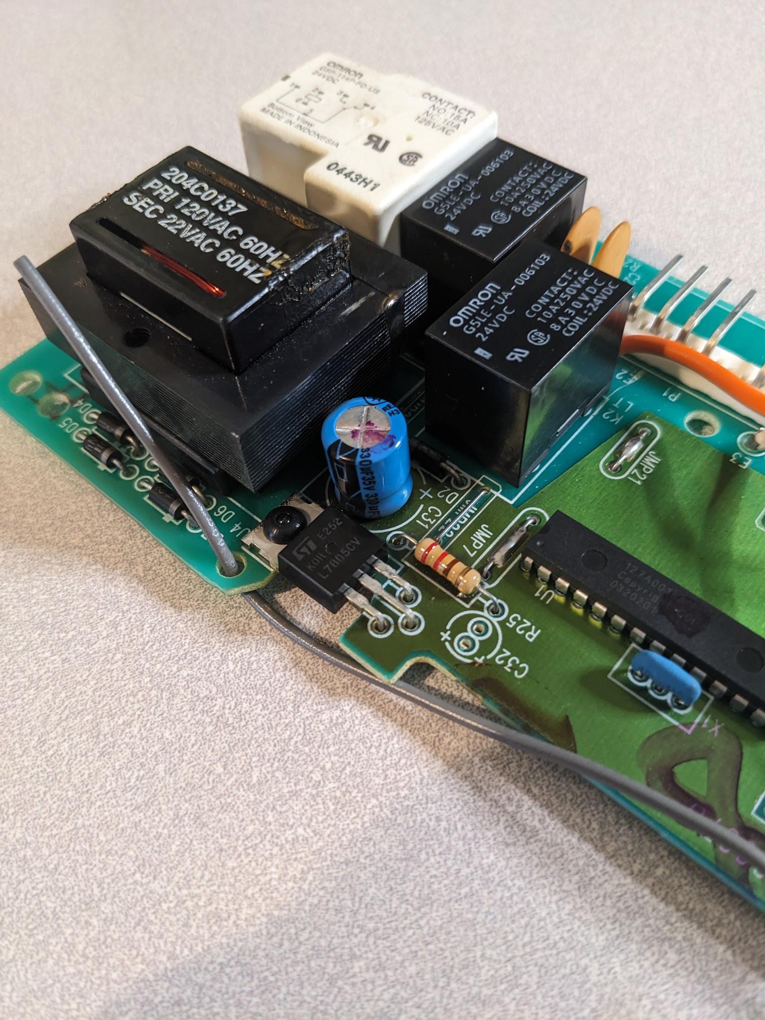
When I tested the “MOSFET” I found that it was actually a voltage regulator. I decided to use it in my circuit to convert the 12v input I would use for the LEDs to 5v that I could use to power the ESP32. This meant I only needed the one 12v input I could get from a wall plug that came with the LEDs.
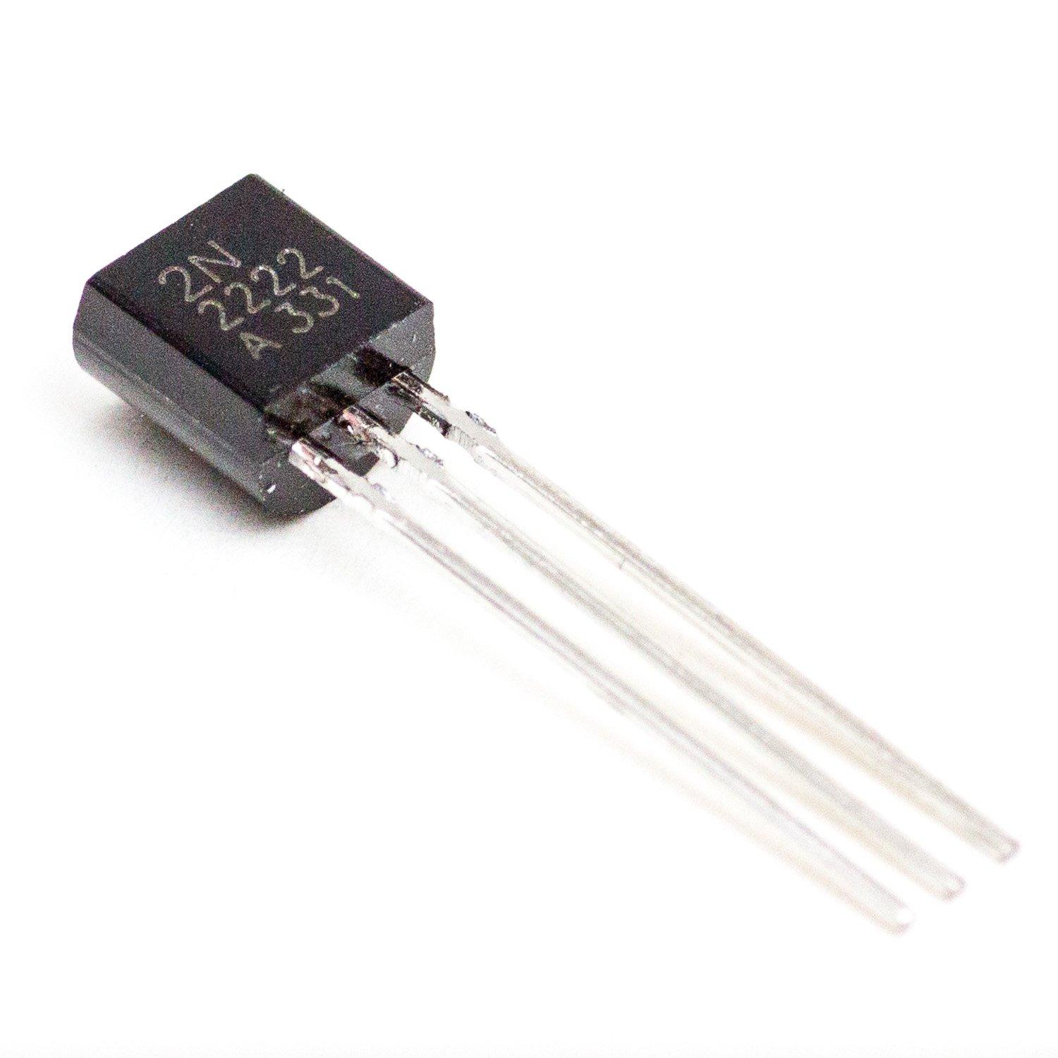
Without the MOSFET I needed something to allow the ESP32 to control the 12v power going to the LEDs. I had some small 2N2222A transistors that (based on a google search) could theoretically supply enough current to the LEDs. However, when I put the 2N2222A transistor into my circuit and tested it, it was not able to power the LEDs. (I expected this, though wanted to test it.) I would need a different way to power the LEDs.
Without the MOSFET I needed something to allow the ESP32 to control the 12v power going to the LEDs. I had some small 2N2222A transistors that (based on a google search) could theoretically supply enough current to the LEDs. However, when I put the 2N2222A transistor into my circuit and tested it, it was not able to power the LEDs. (I expected this, though wanted to test it.) I would need a different way to power the LEDs.
I then decided to use a relay to control the voltage going into the LEDs. It would certainly be able to supply the current needed by the 360 UV LEDs.
Unfortunately, I used my only low voltage relay in the water wheel project so I would need to wait until Monday to pick it up from school. After I picked it up and wired it into my circuit, I realized that the ESP32 could not supply the 5v out of its GPIO pins to power the relay. I then wired up a 2N2222A transistor to take 5v from the power going into the ESP32 and turn on the relay with a control signal from the ESP32.

The UV Light Box (Software):
With the UV light box fully assembled I needed software for it. I thought it would be cool to have the UV light box controlled through a website.
I programmed the ESP32 to connect to my home network and host a website. The website worked by redirecting after a second to the IP address of the ESP32 (Usually 10.0.0.3 on my home network). This allowed me to display new information every second.
Some of the code is on the right:
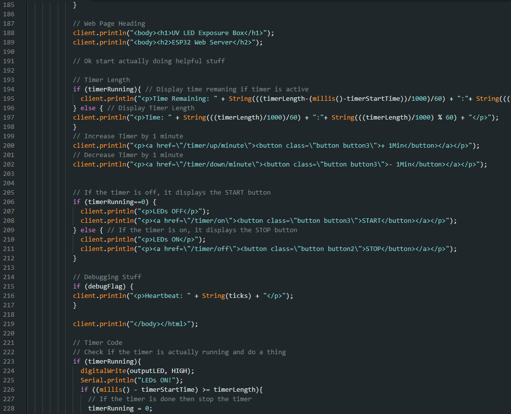
To add inputs to the website I added buttons that made requests to certain file locations on the website. I could then read what file locations were being requested and take that as an input. I used this to control the timer length and whether the LEDs timer was on or off.
On the right is a video of the ESP32 website on my home network and the electronics:
The Game Console:
This was the part where I would attempt to create a PCB using the UV light box I had created. I had never used PCB design software before so all of this was new for me.
My goal for this was to create a small game console powered by a ATTINY85 microprocessor.
I got inspiration from an Electronoobs video about this console that can be found here.
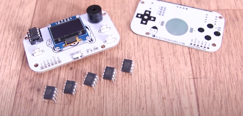
His finished product (professionally made):
The Game Console (Designer):
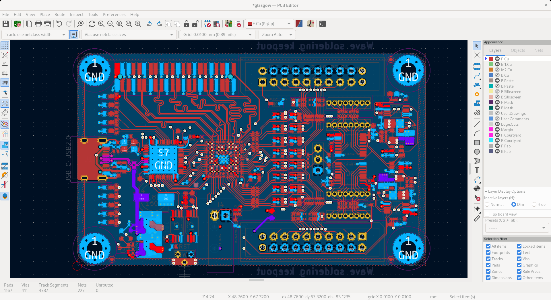
I chose KiCad as my PCB design software because is was a free (and open source) platform that was recommended for people starting out in PCB design.
Example PCB in KiCad:

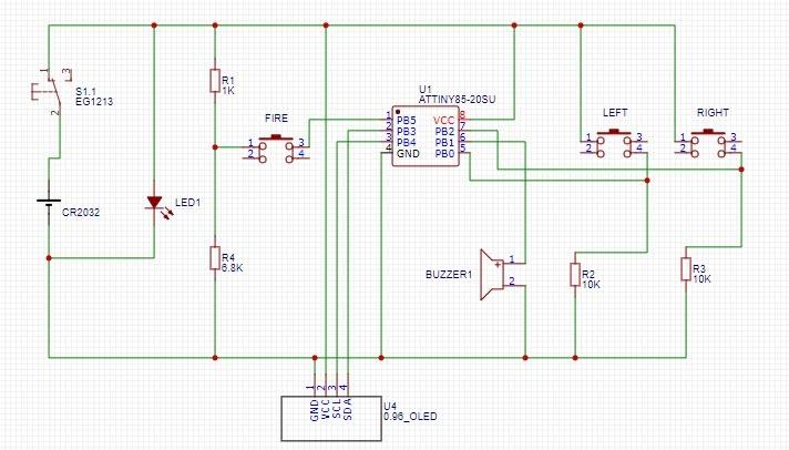
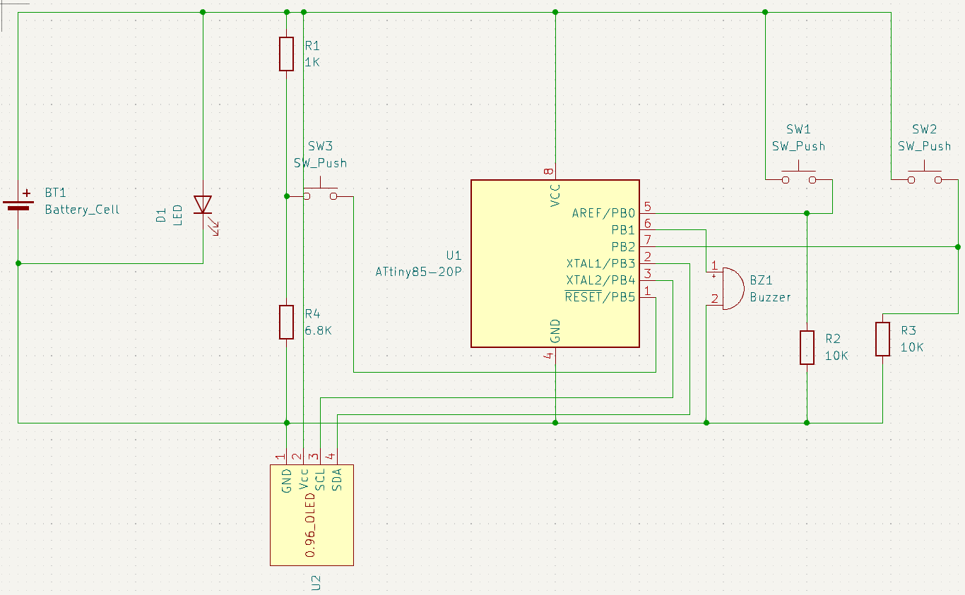
The Game Console (Schematic):
After a bit of searching I was able to find a picture of the schematic diagram for the ATTINY85 game console (top). I then created my version of this schematic diagram in KiCad. As this was my first time it took a little while, but I was able to get everything I needed. This involved creating some components in KiCad that were not there by default. One of these components was my 0.96in OLED screen.
My completed schematic diagram is the bottom image.
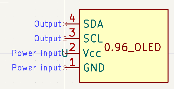
Creating a component for my 0.96in OLED screen.
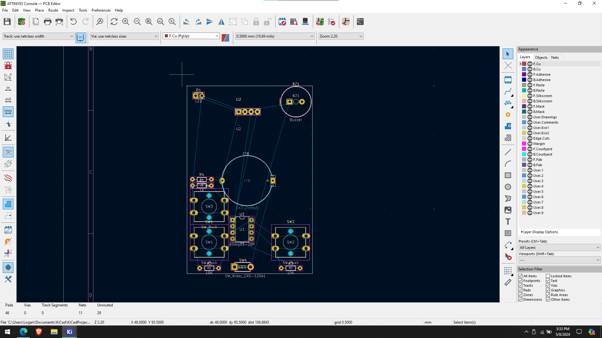
The Game Console (Layout):
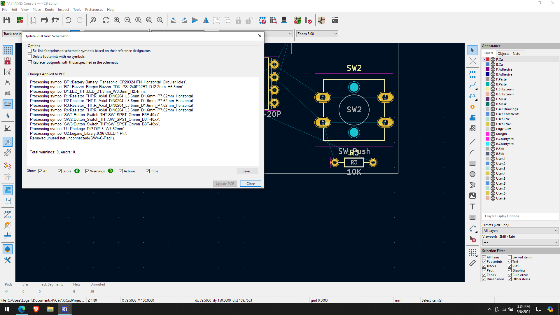
When I jumped into the layout part of my PCB design I was not aware that I needed to apply a footprint to every object in the schematic. This meant that for a while I didn't have every component showing up or the wrong components would be showing up. Eventually I found how to set the schematic footprints. I also designed footprints for my custom components.
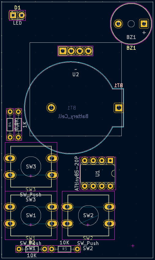
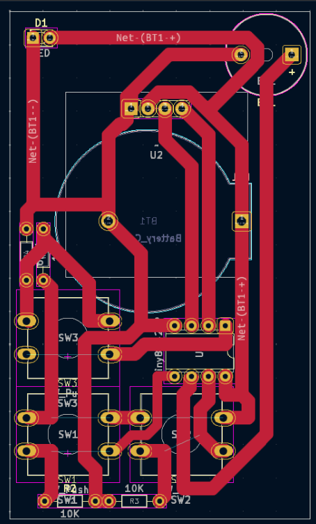
On the left you can see my initial layout for the components. I moved them around a bit for my final layout (right) as I realized I could save some space. I ended up with the board dimensions of 3 inches long by 1.771 inches wide. I also removed the switch as I realized I didn't have a good one on hand and it would be pretty easy to just take out the battery when not using the console.
On the bottom is an image of no errors after I corrected the footprints for all schematic components.
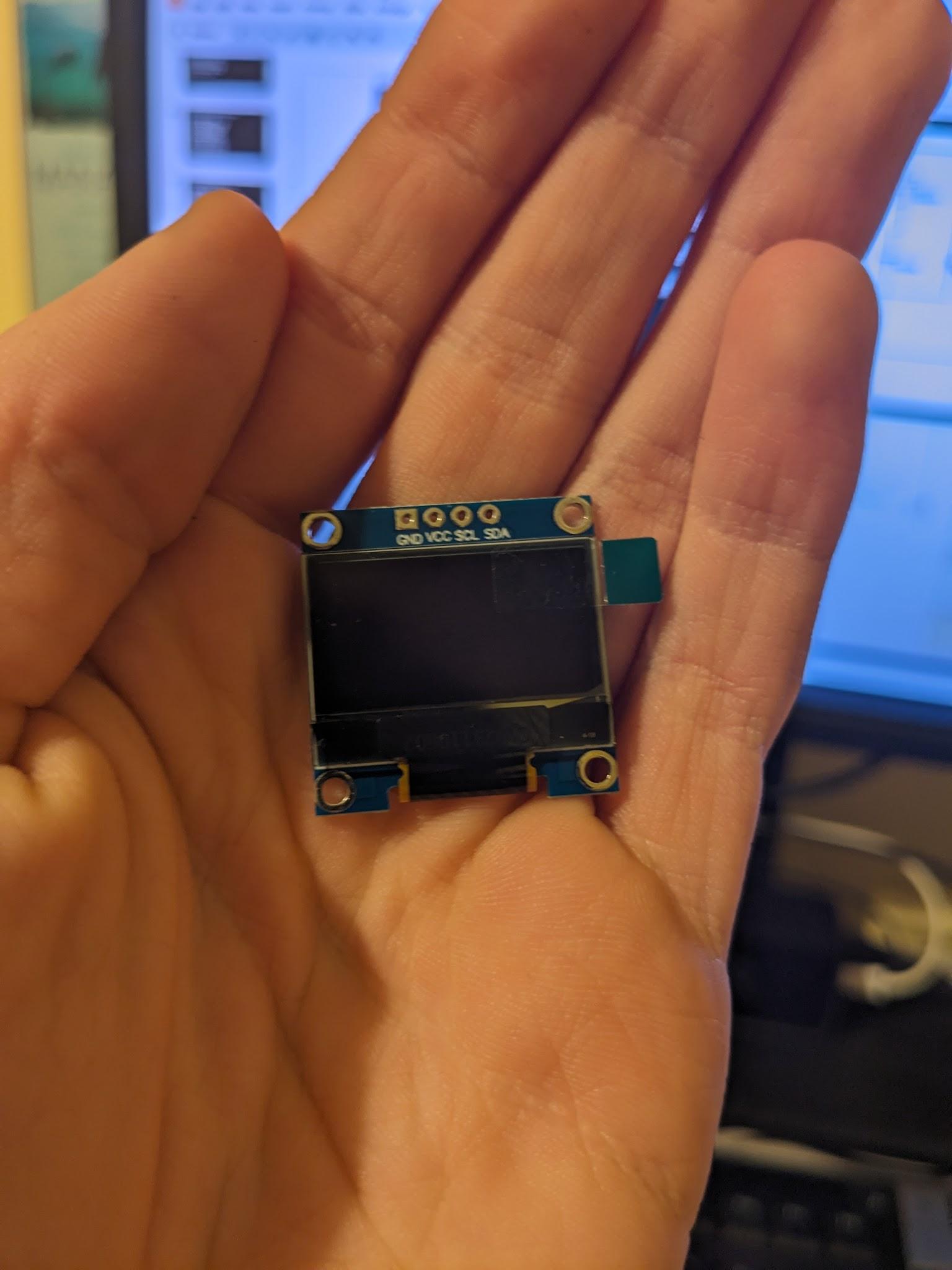
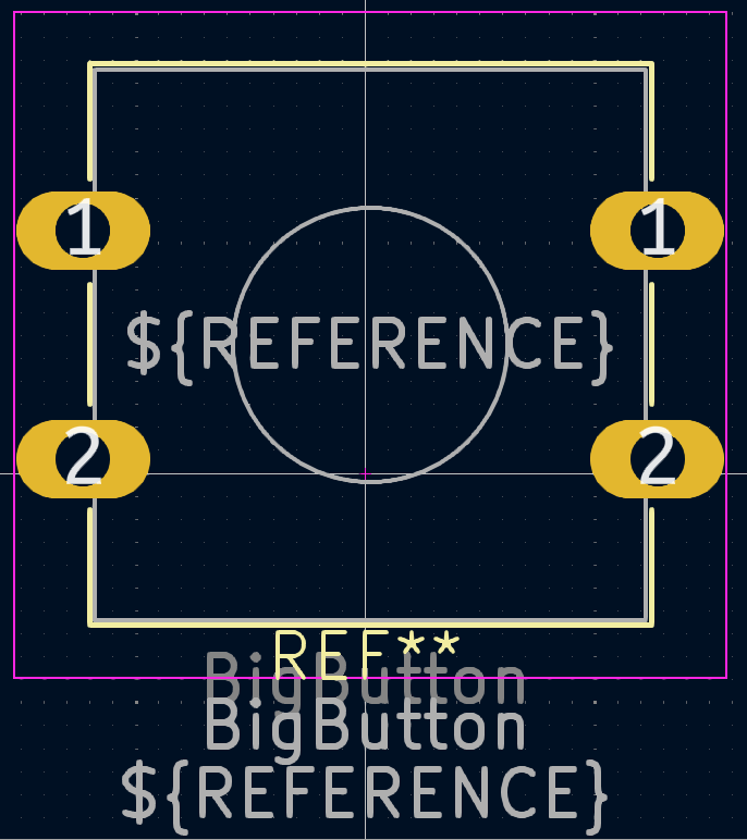
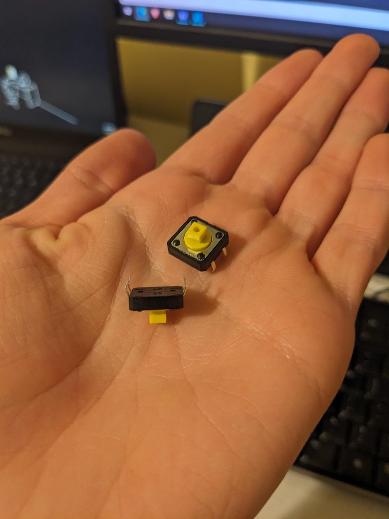
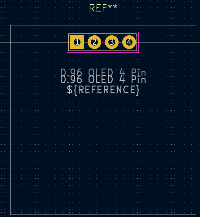
Here are screenshots of the 2 custom footprints I created for my PCB along with pictures of the actual components:
The buttons I used in this project are the same buttons I used in my retro gaming controller project (my previous makerspace).
The pink lines in the footprints are no-go zones where other components cannot be placed.
The white space around the OLED module represents the space it would take up. I used this instead of a no-go zone because I could still place small parts behind / under the OLED module I just needed to know how to fit everything together.

The Game Console (Traces):
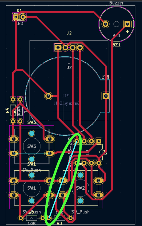
I then traced out all of the copper traces that would connect the components of my PCB. I started with thin traces at first but this looked a bit odd so I redesigned the traces with thicker lines that connected everything. On the first iteration, the 2 resistors at the bottom were also not connected to GND. (You can see this in the picture on the right / small blue wire connecting straight from resistors to a GND pad.) In my revision while making the line traces thicker I realized that some traces between the buttons were unnecessary as the buttons would complete those traces. (The ratlines / PCB planning lines did not know this and traced between them.)
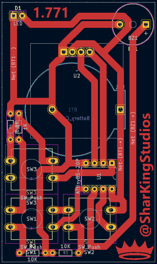
On the left is the first iteration of the line traces and on the right is the almost final version of the traces. (I only made a very minor change in the final version.)
The Game Console (Final Touches):
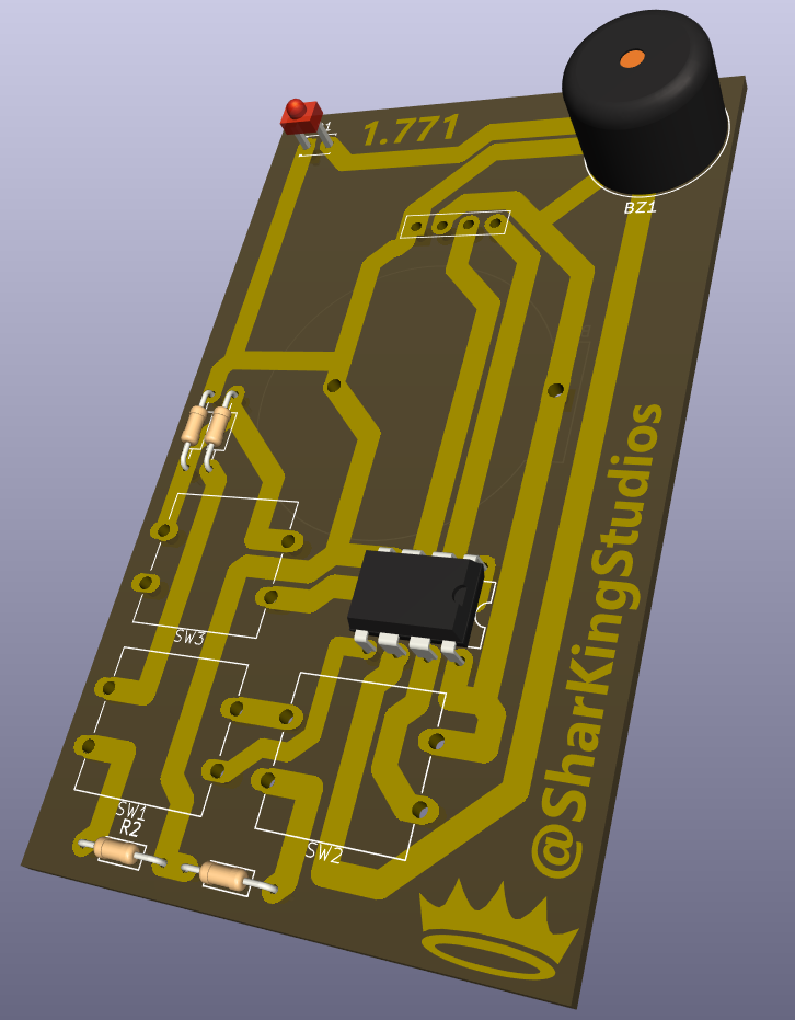
My final version of the PCB design added some text to my youtube channel and its logo. I also added some text for the notable size of the console at 1.771 inches wide. (Such a sneaky robotics reference.) In this 3D viewer the colors are a bit odd after I removed a masking layer. That masking layer is the green top to most PCBs but that would not be present on my homemade PCB. The odd yellow layer would be a shiny copper. The 3D view is also missing models for some of the items. I was not interested in finding how to add my own models as that seemed like an unnecessary amount of work for some aesthetics (and it was a small part of the project).
Attempting to make the PCB:
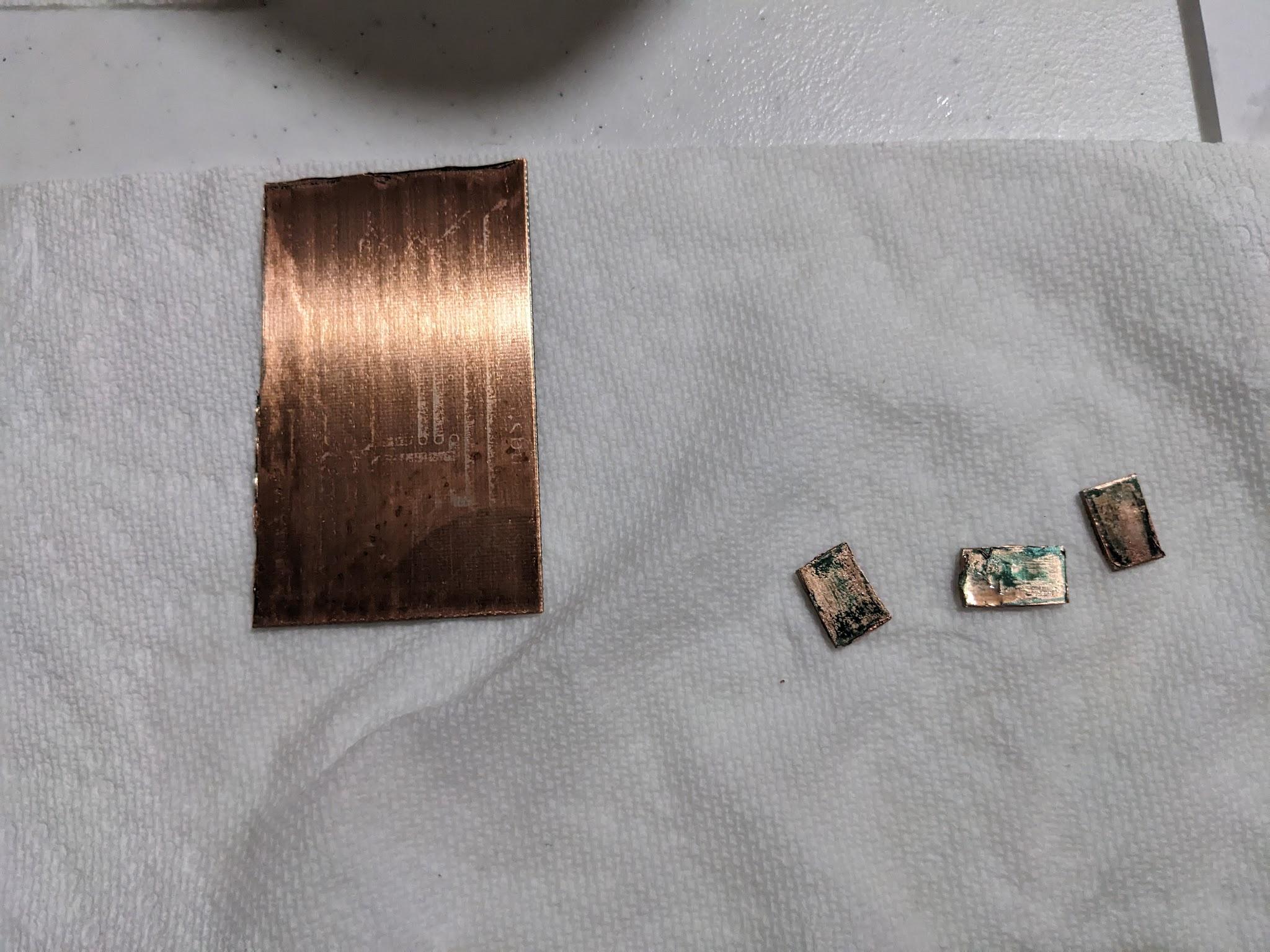
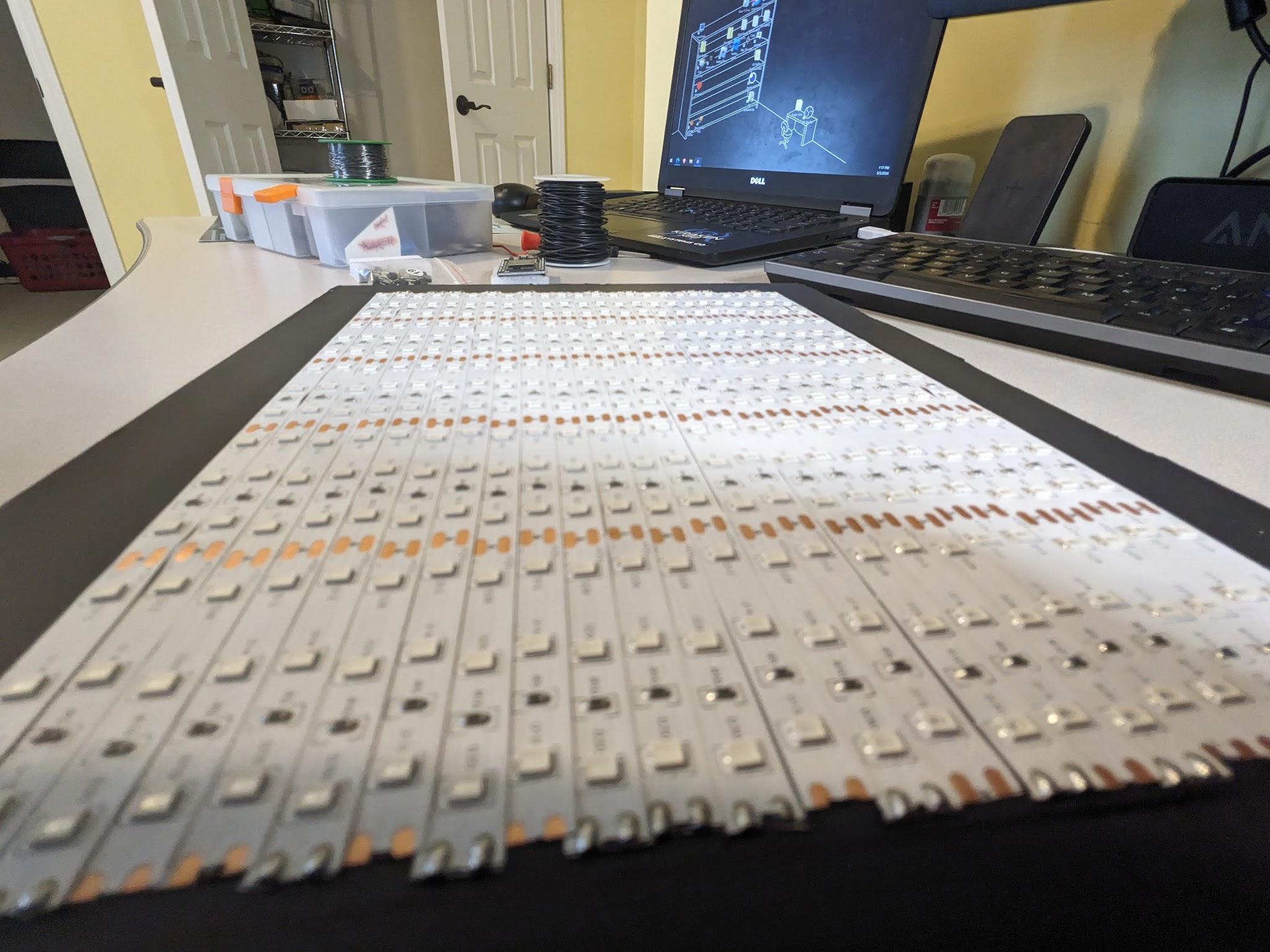
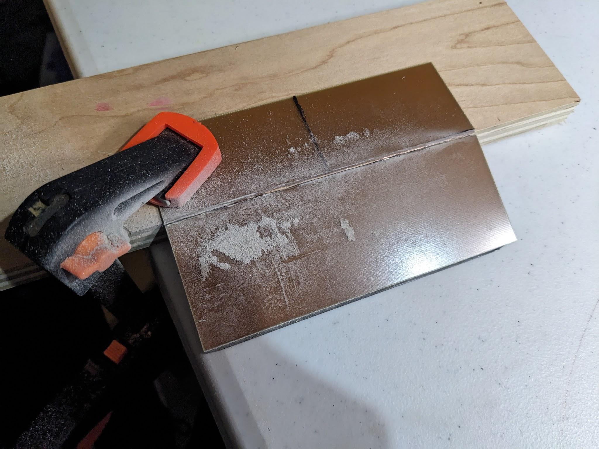
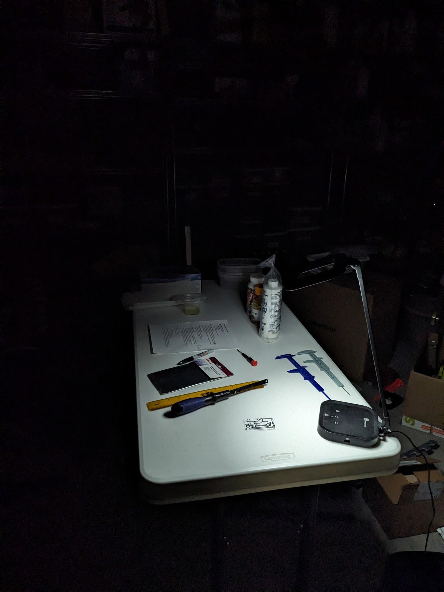
With all the design files finalized I had everything I needed to create the PCBs. (I bought all of the chemicals I would need in PCB fabrication.)
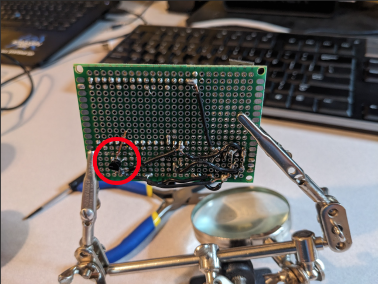
I worked in a dim environment because the photoresist is sensitive to UV light. I started by cutting the PCB with a dremel tool. I then put some cooking oil over the photoresist on the PCB (to convert my regular paper into parchment paper and to stick to the PCB). The paper would have the pattern I want to put on the PCB. I would then expose the PCB in my UV LED Light Box for a couple of minutes. I would then develop the PCB by placing it in a Lye and water solution. This would remove the photoresist that got developed in the UV step. I did not successfully get past this step.
Final Reflection:
While my initial tests ultimately led to a failure I have some PCB material left so I can make some more small test pieces before I create the whole console PCB. This was my second most expensive project this year, beat by the entire FRC robot base that I built during the first makerspace. I bought around $30 of electronics components from Mouser Electronics and around $60 of parts from Amazon for this project.
This project will allow me to fabricate PCBs cheaper then having them professionally done in China and shipped over to the US. Once I get all of the parameters dialed in for my setup I should be able to create PCBs relatively easily. One of the great things about this project was learning how to use KiCad. I will continue to use PCB design softwares like it for (I think) a very long time.
Since I have some PCB material left, I will attempt the PCB design again soon. If the PCBs don't work out, I will put the components onto a protoboard so I can show something soon.
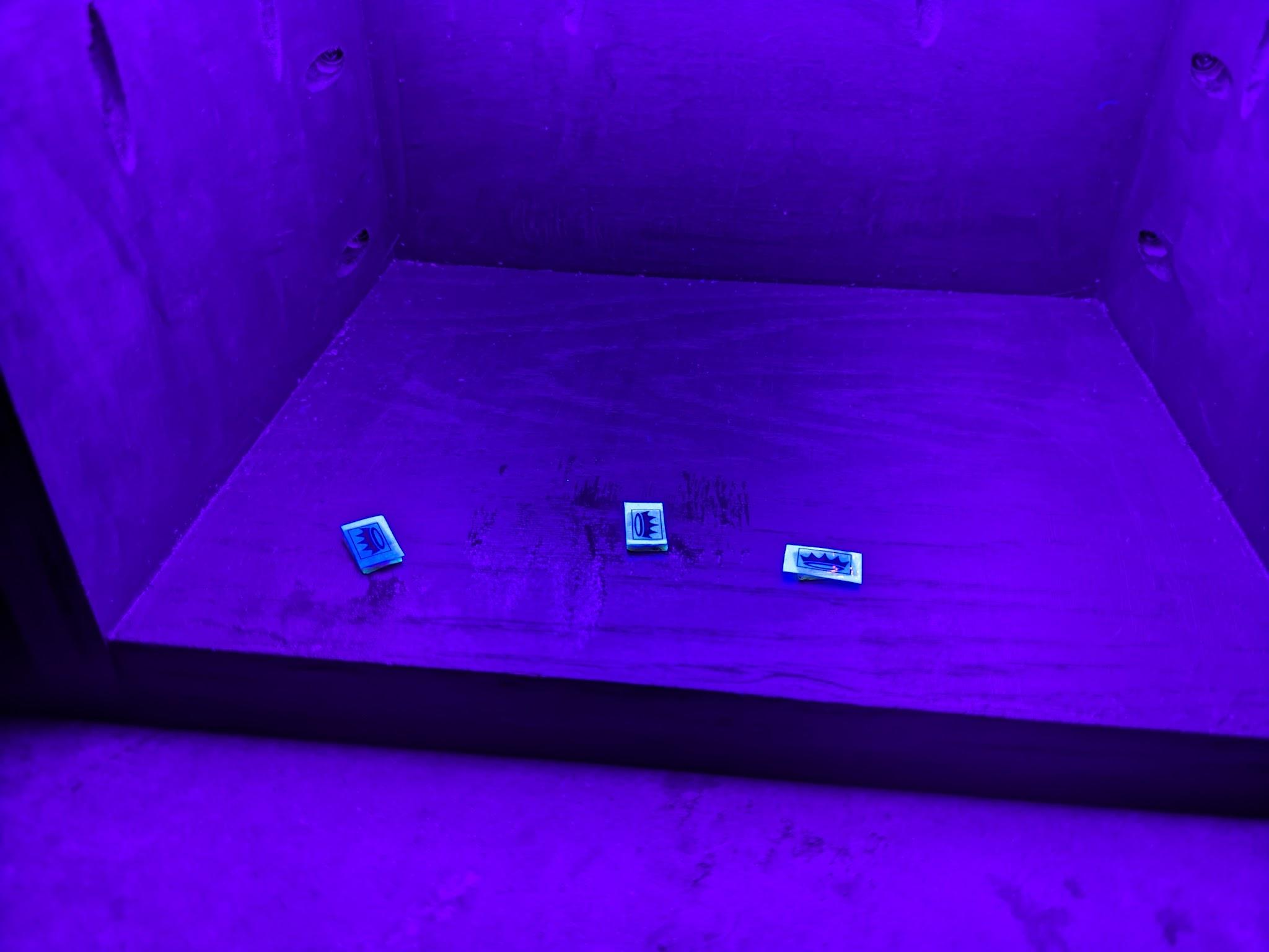
In the picture on the right you can barely make out some of the side text and some of the traces on the board.